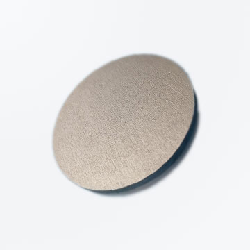
Bismuth Selenide Sputtering Target
AvailableBismuth Selenide Sputtering Target for SaleWholesale & RetailManufacturer & SupplierFactory Supply
Symbol: Bi2Se3Purity: 99.99% - 99.999%Size: 0 - 48 inchThickness: ≥ 1 mmShape: Circular, rectangular, annular, rotary etc.Ships to: Worldwide
Bismuth Selenide Sputtering Target List
| Product Name |
Shape |
Purity |
Size (inch) |
Thickness (mm) |
| Bismuth Selenide Sputtering Target |
Circular |
99.99% - 99.999% |
0 - 48 |
≥ 1 |
| Bismuth Selenide Sputtering Target |
Rectangular |
99.99% - 99.999% |
0 - 48 |
≥ 1 |
| Bismuth Selenide Sputtering Target |
Annular |
99.99% - 99.999% |
0 - 48 |
≥ 1 |
| Bismuth Selenide Sputtering Target |
Oval |
99.99% - 99.999% |
0 - 48 |
≥ 1 |
| Bismuth Selenide Sputtering Target |
Cylindrical |
99.99% - 99.999% |
0 - 48 |
≥ 1 |
| Bismuth Selenide Sputtering Target |
Planar |
99.99% - 99.999% |
0 - 48 |
≥ 1 |
| Bismuth Selenide Sputtering Target |
Rotatable (rotary) |
99.99% - 99.999% |
0 - 48 |
≥ 1 |
Note: We provide customized service. If you don't find the sputtering targets you want, please send us an email directly. We can customize it according to your requirements.
Bismuth selenide is a kind of selenide with rhombohedral crystal structure. The chemical formula is Bi2Se3. The density is 6.82 g / cm3. The melting point is 710 ℃. Bismuth selenide is insoluble in alkali and easily decomposed by concentrated acid and aqua regia. Bismuth selenide is prepared by the direct reaction of selenium and bismuth or the reaction of bismuth oxide and hydrogen selenide.
Bismuth selenide sputtering target is a kind of high purity bismuth selenide raw material by sputtering deposition. According to the different shapes, bismuth selenide sputtering targets can be divided into circular, rectangular, square, annular, oval, cylindrical, planar, rotatable (rotary) bismuth selenide targets. Bismuth selenide can be used as semiconductor material and thermoelectric material.
Bismuth Selenide Sputtering Target Application
High purity bismuth selenide sputtering target can be used in many applications. The details are as follows:
- Semiconductor;
- Chemical vapor deposition (CVD) display;
- Physical vapor deposition (PVD) display;
- Optical applications.
