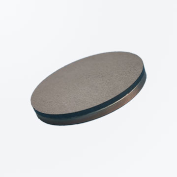
Indium Selenide Sputtering Target
AvailableIndium Selenide Sputtering Target for SaleWholesale & RetailManufacturer & SupplierFactory Supply
Symbol: In2Se3Purity: 99.99% - 99.999%Size: 0 - 48 inchThickness: ≥ 1 mmShape: Circular, rectangular, annular, rotary etc.Ships to: Worldwide
Indium Selenide Sputtering Target List
| Product Name |
Shape |
Purity |
Size (inch) |
Thickness (mm) |
| Indium Selenide Sputtering Target |
Circular |
99.99% - 99.999% |
0 - 48 |
≥ 1 |
| Indium Selenide Sputtering Target |
Rectangular |
99.99% - 99.999% |
0 - 48 |
≥ 1 |
| Indium Selenide Sputtering Target |
Annular |
99.99% - 99.999% |
0 - 48 |
≥ 1 |
| Indium Selenide Sputtering Target |
Oval |
99.99% - 99.999% |
0 - 48 |
≥ 1 |
| Indium Selenide Sputtering Target |
Cylindrical |
99.99% - 99.999% |
0 - 48 |
≥ 1 |
| Indium Selenide Sputtering Target |
Planar |
99.99% - 99.999% |
0 - 48 |
≥ 1 |
| Indium Selenide Sputtering Target |
Rotatable (rotary) |
99.99% - 99.999% |
0 - 48 |
≥ 1 |
Note: We provide customized service. If you don't find the sputtering targets you want, please send us an email directly. We can customize it according to your requirements.
Indium selenide is a compound of indium and selenium. It has potential for use in photovoltaic devices. The two most common phases, α and β, have a layered structure, while γ is a "defect wurtzite structure." In all, there are five known forms (α, β, γ, δ, κ). The α- β phase transition is accompanied by a change in electrical conductivity. The band-gap of γ-In2Se3 is approximately 1.9 eV.
Indium selenide sputtering target is a kind of high purity indium selenide raw material by sputtering deposition. According to the different shapes, indium selenide sputtering targets can be divided into circular, rectangular, square, annular, oval, cylindrical, planar, rotatable (rotary) indium selenide targets.
Indium Selenide Sputtering Target Application
High purity indium selenide sputtering target can be used in many applications. The details are as follows:
- Semiconductor;
- Chemical vapor deposition (CVD) display;
- Physical vapor deposition (PVD) display;
- Optical applications.
