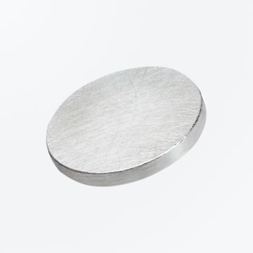
Indium Sputtering Target
AvailableIndium Sputtering Target for SaleWholesale & RetailManufacturer & SupplierFactory Supply
Symbol: InPurity: 99.99% - 99.999%Size: 0 - 48 inchThickness: ≥ 1 mmShape: Circular, rectangular, annular, rotary etc.Ships to: Worldwide
Indium Sputtering Target List
| Product Name |
Shape |
Purity |
Size (inch) |
Thickness (mm) |
| Indium Sputtering Target |
Circular |
99.99% - 99.999% |
0 - 48 |
≥ 1 |
| Indium Sputtering Target |
Rectangular |
99.99% - 99.999% |
0 - 48 |
≥ 1 |
| Indium Sputtering Target |
Annular |
99.99% - 99.999% |
0 - 48 |
≥ 1 |
| Indium Sputtering Target |
Oval |
99.99% - 99.999% |
0 - 48 |
≥ 1 |
| Indium Sputtering Target |
Cylindrical |
99.99% - 99.999% |
0 - 48 |
≥ 1 |
| Indium Sputtering Target |
Planar |
99.99% - 99.999% |
0 - 48 |
≥ 1 |
| Indium Sputtering Target |
Rotatable (rotary) |
99.99% - 99.999% |
0 - 48 |
≥ 1 |
Note: We provide customized service. If you don't find the sputtering targets you want, please send us an email directly. We can customize it according to your requirements.
Indium is a silvery white and bluish metal. The element symbol is In. The melting point is 157 ℃. The boiling point is 2060 ℃. The relative density is 7.30. Indium is malleable and can be pressed into sheets. Indium is mainly used as raw material for manufacturing low melting alloy, bearing alloy, semiconductor, electric light source, etc.
Indium sputtering target is a kind of high purity indium raw material by sputtering deposition. According to the different shapes, indium sputtering targets can be divided into circular, rectangular, square, annular, oval, cylindrical, planar, rotatable (rotary) indium targets. Indium has strong light permeability and conductivity, and is mainly used in the production of ITO targets (for LCD and flat screen). It is widely used in electronic semiconductor, solder and alloy, scientific research, medicine and other fields.
Indium Sputtering Target Application
High purity indium sputtering target produced by FUSHEL has the highest possible density and smallest possible average grain sizes. It can be used in many applications. The details are as follows:
- Electronics;
- Semiconductor;
- Flat panel displays.
