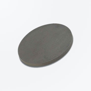
Molybdenum Carbide Sputtering Target
AvailableMolybdenum Carbide Sputtering Target for SaleWholesale & RetailManufacturer & SupplierFactory Supply
Symbol: Mo2CPurity: 99.5% - 99.9%Size: 0 - 48 inchThickness: ≥ 1 mmShape: Circular, rectangular, annular, rotary etc.Ships to: Worldwide
Molybdenum Carbide Sputtering Target List
| Product Name |
Shape |
Purity |
Size (inch) |
Thickness (mm) |
| Molybdenum Carbide Sputtering Target |
Circular |
99.5% - 99.9% |
0 - 48 |
≥ 1 |
| Molybdenum Carbide Sputtering Target |
Rectangular |
99.5% - 99.9% |
0 - 48 |
≥ 1 |
| Molybdenum Carbide Sputtering Target |
Annular |
99.5% - 99.9% |
0 - 48 |
≥ 1 |
| Molybdenum Carbide Sputtering Target |
Oval |
99.5% - 99.9% |
0 - 48 |
≥ 1 |
| Molybdenum Carbide Sputtering Target |
Cylindrical |
99.5% - 99.9% |
0 - 48 |
≥ 1 |
| Molybdenum Carbide Sputtering Target |
Planar |
99.5% - 99.9% |
0 - 48 |
≥ 1 |
| Molybdenum Carbide Sputtering Target |
Rotatable (rotary) |
99.5% - 99.9% |
0 - 48 |
≥ 1 |
Note: We provide customized service. If you don't find the sputtering targets you want, please send us an email directly. We can customize it according to your requirements.
Molybdenum carbide is a kind of gray carbide in appearance. The chemical formula is MoC and the molecular weight is 107.95. The melting point is 2692 ℃. Molybdenum carbide is insoluble in water and alkali, but slightly soluble in nitric acid, sulfuric acid and hydrofluoric acid.
Molybdenum carbide sputtering target is a kind of high purity molybdenum carbide raw material by sputtering deposition. According to the different shapes, molybdenum carbide sputtering targets can be divided into circular, rectangular, square, annular, oval, cylindrical, planar, rotatable (rotary) molybdenum carbide targets. Molybdenum carbide has high melting point and hardness, good thermal and mechanical stability and good corrosion resistance. It can be used in electronics, metal processing and aerospace industry.
Molybdenum Carbide Sputtering Target Application
Molybdenum carbide sputtering target can be used in many applications. The details are as follows:
- Semiconductor;
- Chemical vapor deposition (CVD) display;
- Physical vapor deposition (PVD) display;
- Optical applications.
