Aluminum Sputtering Target List
| Product Name |
Shape |
Purity |
Size (inch) |
Thickness (mm) |
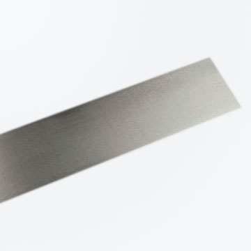
| Aluminum Sputtering Target |
Circular |
99.99% - 99.9995% |
0 - 48 |
≥ 1 |
| Aluminum Sputtering Target |
Rectangular |
99.99% - 99.9995% |
0 - 48 |
≥ 1 |
| Aluminum Sputtering Target |
Annular |
99.99% - 99.9995% |
0 - 48 |
≥ 1 |
| Aluminum Sputtering Target |
Oval |
99.99% - 99.9995% |
0 - 48 |
≥ 1 |
| Aluminum Sputtering Target |
Cylindrical |
99.99% - 99.9995% |
0 - 48 |
≥ 1 |
| Aluminum Sputtering Target |
Planar |
99.99% - 99.9995% |
0 - 48 |
≥ 1 |
| Aluminum Sputtering Target |
Rotatable (rotary) |
99.99% - 99.9995% |
0 - 48 |
≥ 1 |
Note: We provide customized service. If you don't find the sputtering targets you want, please send us an email directly. We can customize it according to your requirements.
Aluminum is a kind of silver white light metal with ductility. Aluminum is often made into rod, sheet, foil, powder, ribbon and wire. It can form an oxide film to prevent metal corrosion in humid air. Aluminum is easily soluble in dilute sulfuric acid, nitric acid, hydrochloric acid, sodium hydroxide and potassium hydroxide solutions, but not in water. The relative density of aluminum is 2.70. The melting point is 660 ℃. The boiling point is 2327 ℃.
High-purity aluminum sputtering target material is a key raw material used in physical vapor deposition (PVD) processes for sputter coating. It is defined as a solid target material with an aluminum purity typically no lower than 99.99% (4N). When bombarded by high-energy particles (such as argon ions) in a vacuum environment, its surface atoms or molecules are ejected and deposited onto a substrate (such as a silicon wafer or glass substrate), forming a layer of aluminum or aluminum alloy thin film with specific functions.
Core Value and Importance
In high-end manufacturing fields like semiconductors and display panels, the performance of the thin film directly determines the electrical, optical, and reliability properties of the final product. As the "source" of the thin film, the purity, microstructure, density, and internal defects of the target directly "inherit" into the thin film. Therefore, high-purity aluminum sputtering targets are not ordinary aluminum materials but high-tech, precision-manufactured functional materials with high added value. They are an indispensable link in the semiconductor manufacturing supply chain.
Classification
High-purity
aluminum sputtering targets can be classified in multiple dimensions according to purity, microstructure, geometric shape, and bonding method.
1. Classification by Purity Grade:Purity is the most critical classification criterion, as it directly affects the resistivity, impurity defect density, and the performance and yield of the final device.
4N5 (99.995%): Applied in fields that require strict impurity control, such as electrodes in some high-resolution display panels.
5N (99.999%): The mainstream standard for semiconductor integrated circuit manufacturing. Used for metal interconnections, via plugs, and other components in advanced process nodes ranging from 90nm to 28nm and beyond. This ensures low contact resistance and excellent electromigration reliability.
6N (99.9999%) and above: Used in ultra-high-end semiconductor devices, compound semiconductors, and cutting-edge memory devices (e.g., 3D NAND). The impurity content at this purity level is close to the detection limit, aiming to minimize impurity defects in the thin film, meeting the needs of processes below 10nm.
2. Classification by Microstructure and Preparation Process:The microstructure determines the sputtering rate, thin film uniformity, and particle contamination level.
Forged Targets: Made by high-temperature forging, which refines the grain structure and densifies the material. The advantages are uniform grain structure and excellent mechanical properties. This was the mainstream process in the past.
Rolled Targets: Obtained through multiple rolling passes. The grain orientation is relatively strong, and the cost is lower. This is suitable for applications that require specific orientation control.
Hot Isostatic Pressing (HIP) Targets: Manufactured using powder metallurgy combined with HIP technology. It allows near-net shaping, extremely uniform microstructure, and eliminates macroscopic segregation. This is especially suitable for large-sized targets (e.g., for G8.5 and larger display panels) and custom-shaped targets, and is the current mainstream for high-end applications.
3. Classification by Final Product Shape:Monolithic Targets: Entirely made from a single material (high-purity aluminum or aluminum alloy).
Bonded Targets: To save on expensive target material and ensure good heat dissipation, the target material (or target blank) is permanently bonded with a backing plate (usually made from oxygen-free copper or aluminum) through diffusion bonding or brazing techniques. This is the standard form for semiconductor targets, requiring high bonding rates (>95%), good thermal conductivity, and no cracking under thermal stress.
Planar Targets: The most common flat or round targets, typically used in various PVD applications.
Rotary Targets (Cylindrical Targets): Hollow cylindrical shape, continuously rotating during sputtering. The utilization rate can exceed 80% (compared to 20-40% for planar targets), providing excellent film thickness uniformity. These are widely used for large-area coatings, such as in flat-panel displays, architectural coating glass, and solar cells.
Aluminum Sputtering Target Application
High-purity aluminum sputtering targets are deeply integrated into various core sectors of modern electronics and information industries.
1. Semiconductor Integrated Circuit (IC) Manufacturing:This is the most critical and technically demanding application.
Metal Interconnections and Via Plugs: Aluminum thin films (often alloyed with copper or silicon) are used as "wires" connecting billions of transistors within chips. Aluminum plugs are used to fill micro-holes, ensuring inter-layer connections. The thin film must exhibit ultra-low resistivity, excellent step coverage, and high resistance to electromigration.
Bonding Pads: These metal regions on the chip surface provide the interface for external gold bonding wires, requiring the film to have good adhesion, bondability, and corrosion resistance.
Gate Electrode: In some processes or devices, aluminum is used as the gate material.
2. Flat Panel Displays (FPD):Thin-Film Transistor Liquid Crystal Displays (TFT-LCD): Used to create the source, drain, and data lines in the TFT array. As display resolution (4K/8K) increases, the aluminum targets require lower resistivity to reduce signal delay. Rotary targets are often used for large-size substrates (such as G10.5 glass substrates) and higher utilization rates.
Organic Light Emitting Diode (OLED): Used for anode modification layers, circuit interconnections, etc. The purity and film quality of the target must be extremely high, as tiny particle defects can cause OLED pixel failure.
Touch Panels: Used to form metal lines beneath transparent conductive oxide (such as ITO) films, serving as auxiliary electrodes to reduce overall resistance.
3. Solar Energy (Photovoltaic) Industry:Crystalline Silicon Solar Cells: Aluminum films are sputtered onto the back of the cell to form back surface fields (BSF) or passivated contact layers (such as in PERC technology). This helps reflect charge carriers, improving open-circuit voltage and conversion efficiency. This application uses large volumes of material, with cost sensitivity, typically employing 4N-5N purity flat or rotary targets.
Thin-Film Solar Cells (e.g., CIGS): Used for back electrodes or interconnection wires in the modules.
4. Data Storage Disks:Used for manufacturing aluminum alloy substrates for hard disk platters (e.g., glass substrates), requiring extremely smooth, defect-free surfaces. With increasing storage capacities, the demands for substrate flatness and target purity are rising.
5. Other High-End Applications:Optical Components: Sputtered aluminum films are used for high-reflectivity layers in precision optical lenses and mirrors. These require high purity, excellent reflectivity, and minimal defects in the film.
Decorative and Functional Coatings: Used for wear-resistant decorative coatings on mobile phone frames, watch cases, and hard-wearing layers on tools.
Semiconductor Packaging: In advanced packaging technologies, used to prepare re-routing layers (RDL) or metalized bumps under bump metallization (UBM) layers.