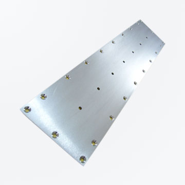
Nickel Sputtering Target
AvailableNickel Sputtering Target for SaleWholesale & RetailManufacturer & SupplierFactory Supply
Symbol: NiPurity: 99.9% - 99.999%Size: 0 - 48 inchThickness: ≥ 1 mmShape: Circular, rectangular, annular, rotary etc.Ships to: Worldwide
Nickel Sputtering Target List
| Product Name |
Shape |
Purity |
Size (inch) |
Thickness (mm) |
| Nickel Sputtering Target |
Circular |
99.9% - 99.999% |
0 - 48 |
≥ 1 |
| Nickel Sputtering Target |
Rectangular |
99.9% - 99.999% |
0 - 48 |
≥ 1 |
| Nickel Sputtering Target |
Annular |
99.9% - 99.999% |
0 - 48 |
≥ 1 |
| Nickel Sputtering Target |
Oval |
99.9% - 99.999% |
0 - 48 |
≥ 1 |
| Nickel Sputtering Target |
Cylindrical |
99.9% - 99.999% |
0 - 48 |
≥ 1 |
| Nickel Sputtering Target |
Planar |
99.9% - 99.999% |
0 - 48 |
≥ 1 |
| Nickel Sputtering Target |
Rotatable (rotary) |
99.9% - 99.999% |
0 - 48 |
≥ 1 |
Note: We provide customized service. If you don't find the sputtering targets you want, please send us an email directly. We can customize it according to your requirements.
Nickel is a silvery white metal and the chemical formula is Ni. The density of nickel is 8.902 g / cm3, the melting point is 1453 ℃ and the boiling point is 2732 ℃. Nickel has magnetic properties and good plasticity, corrosion resistance, polishing and corrosion resistance. Nickel is green when dissolved in nitric acid. Nickel is mainly used in alloys (such as nickel steel and nickel silver) and as catalysts.
Nickel sputtering target is a kind of high purity nickel raw material for sputtered deposition. According to the different shapes, nickel sputtering targets can be divided into circular, rectangular, square, annular, oval, cylindrical, planar, rotatable (rotary) nickel targets. It is mainly used in semiconductor and microelectronics industry. Nickel sputtering target is the key material of semiconductor back electrode.
Nickel Sputtering Target Application
The nickel sputtering target produced by us has the characteristics of high density and high purity, and the grain size is uniform. In the process of physical vapor deposition, our nickel sputtering target can obtain films with excellent conductivity and particle minimization. It can be used in semiconductor, chemical vapor deposition (CVD) and physical vapor deposition (PVD) display and optical applications. The details are as follows:
- Semiconductor;
- Chemical vapor deposition (CVD) display;
- Physical vapor deposition (PVD) display;
- Microelectronics industry;
- Optical applications.
